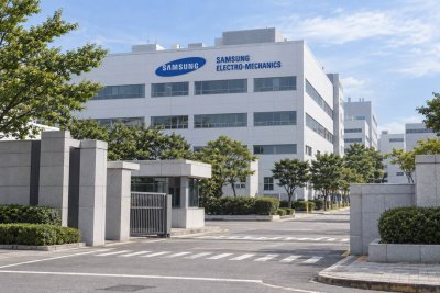
Samsung Electronics has announced a strategic collaboration with ASML aimed at deploying High-NA EUV lithography in high-volume DRAM production by 2028. The partnership also includes Samsung's participation in an industry initiative to develop 12-inch photomasks, a significant departure from the long-standing 6-inch format. While the announcement provides a clear technological roadmap, it does not immediately impact Samsung's 2026 earnings outlook.
Samsung's common shares closed Tuesday at KRW 269,500, down 0.19%, after touching an intraday high of KRW 279,000. The stock had surged 5.68% on Monday, leaving it 5.5% above its September 4 close. Notably, the Seoul market closed at 3:30 p.m. local time before the ASML agreement was widely reported, so Tuesday's closing price serves as a baseline rather than a market reaction to the news.
Technology Roadmap: More Than a Purchase Order
The joint announcement from Samsung and ASML outlines two interconnected steps. First, Samsung will join an industry effort to develop 12-inch photomasks, which offer four times the area of the traditional 6-inch masks. This is particularly relevant because ASML's current High-NA platform uses anamorphic optics that expose a field half the size of conventional EUV systems, requiring multiple exposures for larger chip designs.
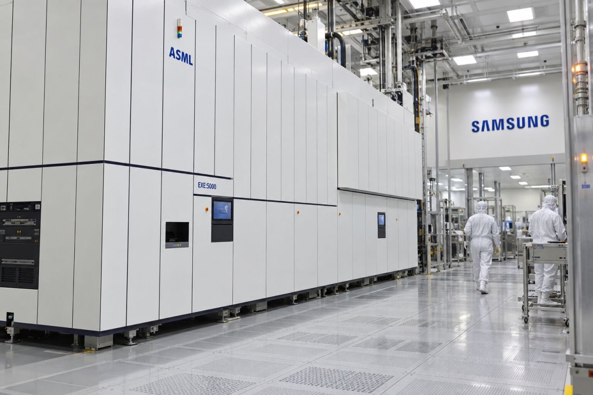
Second, Samsung plans to be the first to use ASML's High-NA EUV equipment (EXE:5000) in high-volume DRAM manufacturing by 2028. High-NA technology increases the numerical aperture from 0.33 to 0.55, enabling 8-nanometer resolution and features 1.7 times smaller than current EUV systems. This could potentially increase transistor density by up to 2.9 times and reduce the need for multiple patterning steps, thereby lowering process complexity and cycle times.
Key Challenges: Ecosystem and Economics
However, the transition to 12-inch masks requires a broader ecosystem—including mask blanks, writers, inspection tools, and handling equipment—that has not yet been fully developed. ASML's EXE:5000 was designed for traditional reticle sizes, so Samsung's initiative depends on industry-wide collaboration. The announcement does not specify a production-readiness date for this ecosystem.
From a financial perspective, Samsung is funding this roadmap from a position of strength. In Q2, the company reported KRW 171.5 trillion in revenue and KRW 89.5 trillion in operating profit, with its Device Solutions division contributing nearly all of the profit. However, this concentration means that a successful High-NA ramp could extend DRAM scaling and protect margins, while a mistimed or costly implementation could add depreciation and complexity just as memory pricing normalizes. Samsung faces intense competition from TSMC in foundry and SK hynix in advanced memory, making capital allocation critical.
Samsung's long-term investment plan earmarks approximately KRW 2,100 trillion for semiconductors between 2026 and 2040, but the company has not disclosed a specific High-NA budget. This lack of detail prevents investors from estimating the return on this particular project.
What Would Make the 2028 Target Investable?
For investors, the key metrics to watch are tool count, DRAM node selection, and whether the reduction in patterning steps offsets the higher equipment and infrastructure costs. Yield data from pilot production—defect density, wafer throughput, and cycle time—will be crucial. Customer qualification, as demonstrated with HBM4 and HBM4E, is another critical factor; a process can be technically ready before major customers validate it and commit volumes.
At Tuesday's close, Samsung's market capitalization stood at approximately KRW 1,575.6 trillion. The stock has gained 5.5% over two sessions, but the ASML disclosure provides no basis for adding a specific premium to the valuation. The next meaningful milestone would be a named DRAM node, a detailed capex plan, or pilot data showing that larger masks and High-NA exposure lower the cost per good die.
Until then, the announcement is best viewed as a credible statement of intent for 2028, leaving the economic burden of proof unchanged.